
Circular Pi Plates - Axial Phase Plates
The circular pi plate, which is also known as an axial phase plate, an annular pi phase plate or a z-doughnut phase mask, imprints a phase shift of π onto a central circular zone of an incident Gaussian laser beam. When the beam is focused, the field from the inner zone and the field from the surrounding ring arrive on the optical axis in antiphase and cancel, so that the focus carries a true intensity zero at its centre and two bright lobes above and below it along the optical axis. This so-called bottle beam or z-doughnut is the axial counterpart of the doughnut produced by a spiral phase plate: the vortex confines light laterally, the circular pi plate confines it axially, and 3D STED microscopy uses both at the same time. Most important properties of a circular pi plate are: accordance to the wavelength and accordance of the zone diameter to the diameter of the incident Gaussian beam. Our circular pi plates show a very small deviation from the theoretical step height (usually ± 5 nm) and a zone diameter tolerance of ± 0.5 %, which places the residual on-axis intensity below 10-3 of the lobe peak. We offer zone diameters of 0.2, 1.0, 2.0 and 3.0 mm for every listed wavelength, so that the plate can be matched to your beam without a telescope. Applications of the circular pi plate include 3D STED, MINFLUX, dark optical traps for cold atoms and nanoparticles, depth-of-focus engineering and laser machining.
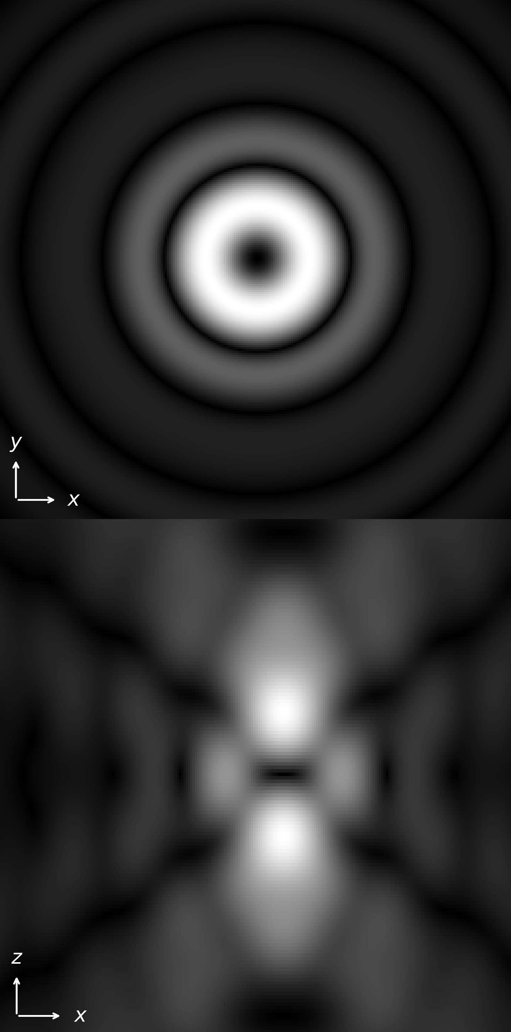
Resulting bottle beam (z-doughnut) in the xz plane after a circular pi plate for 775 nm
Size
All sizesWavelength (λ)
All wavelengthsZone diameter (d)
All diameters| PN | Size | λ | d | Material | Coating/Transm. | Quote | ||
|---|---|---|---|---|---|---|---|---|
|
10 mm aperture |
||||||||
| PiC-405-10-200 |
11x11x2.5 mm |
405 nm |
0.2 mm |
fused silica |
none / 92.91% |
|||
| PiC-405-10-1000 |
11x11x2.5 mm |
405 nm |
1.0 mm |
fused silica |
none / 92.91% |
|||
| PiC-405-10-2000 |
11x11x2.5 mm |
405 nm |
2.0 mm |
fused silica |
none / 92.91% |
|||
| PiC-405-10-3000 |
11x11x2.5 mm |
405 nm |
3.0 mm |
fused silica |
none / 92.91% |
|||
| PiC-488-10-200 |
11x11x2.5 mm |
488 nm |
0.2 mm |
fused silica |
none / 93.14% |
|||
| PiC-488-10-1000 |
11x11x2.5 mm |
488 nm |
1.0 mm |
fused silica |
none / 93.14% |
|||
| PiC-488-10-2000 |
11x11x2.5 mm |
488 nm |
2.0 mm |
fused silica |
none / 93.14% |
|||
| PiC-488-10-3000 |
11x11x2.5 mm |
488 nm |
3.0 mm |
fused silica |
none / 93.14% |
|||
| PiC-532-10-200 |
11x11x2.5 mm |
532 nm |
0.2 mm |
fused silica |
none / 93.14% |
|||
| PiC-532-10-1000 |
11x11x2.5 mm |
532 nm |
1.0 mm |
fused silica |
none / 93.14% |
|||
| PiC-532-10-2000 |
11x11x2.5 mm |
532 nm |
2.0 mm |
fused silica |
none / 93.14% |
|||
| PiC-532-10-3000 |
11x11x2.5 mm |
532 nm |
3.0 mm |
fused silica |
none / 93.14% |
|||
| PiC-592-10-200 |
11x11x2.5 mm |
592 nm |
0.2 mm |
fused silica |
none / 93.07% |
|||
| PiC-592-10-1000 |
11x11x2.5 mm |
592 nm |
1.0 mm |
fused silica |
none / 93.07% |
|||
| PiC-592-10-2000 |
11x11x2.5 mm |
592 nm |
2.0 mm |
fused silica |
none / 93.07% |
|||
| PiC-592-10-3000 |
11x11x2.5 mm |
592 nm |
3.0 mm |
fused silica |
none / 93.07% |
|||
| PiC-640-10-200 |
11x11x2.5 mm |
640 nm |
0.2 mm |
fused silica |
none / 93.41% |
|||
| PiC-640-10-1000 |
11x11x2.5 mm |
640 nm |
1.0 mm |
fused silica |
none / 93.41% |
|||
| PiC-640-10-2000 |
11x11x2.5 mm |
640 nm |
2.0 mm |
fused silica |
none / 93.41% |
|||
| PiC-640-10-3000 |
11x11x2.5 mm |
640 nm |
3.0 mm |
fused silica |
none / 93.41% |
|||
| PiC-660-10-200 |
11x11x2.5 mm |
660 nm |
0.2 mm |
fused silica |
none / 93.37% |
|||
| PiC-660-10-1000 |
11x11x2.5 mm |
660 nm |
1.0 mm |
fused silica |
none / 93.37% |
|||
| PiC-660-10-2000 |
11x11x2.5 mm |
660 nm |
2.0 mm |
fused silica |
none / 93.37% |
|||
| PiC-660-10-3000 |
11x11x2.5 mm |
660 nm |
3.0 mm |
fused silica |
none / 93.37% |
|||
| PiC-775-10-200 |
11x11x2.5 mm |
775 nm |
0.2 mm |
fused silica |
none / 93.29% |
|||
| PiC-775-10-1000 |
11x11x2.5 mm |
775 nm |
1.0 mm |
fused silica |
none / 93.29% |
|||
| PiC-775-10-2000 |
11x11x2.5 mm |
775 nm |
2.0 mm |
fused silica |
none / 93.29% |
|||
| PiC-775-10-3000 |
11x11x2.5 mm |
775 nm |
3.0 mm |
fused silica |
none / 93.29% |
|||
| PiC-780-10-200 |
11x11x2.5 mm |
780 nm |
0.2 mm |
fused silica |
none / 93.33% |
|||
| PiC-780-10-1000 |
11x11x2.5 mm |
780 nm |
1.0 mm |
fused silica |
none / 93.33% |
|||
| PiC-780-10-2000 |
11x11x2.5 mm |
780 nm |
2.0 mm |
fused silica |
none / 93.33% |
|||
| PiC-780-10-3000 |
11x11x2.5 mm |
780 nm |
3.0 mm |
fused silica |
none / 93.33% |
|||
| PiC-800-10-200 |
11x11x2.5 mm |
800 nm |
0.2 mm |
fused silica |
none / 93.33% |
|||
| PiC-800-10-1000 |
11x11x2.5 mm |
800 nm |
1.0 mm |
fused silica |
none / 93.33% |
|||
| PiC-800-10-2000 |
11x11x2.5 mm |
800 nm |
2.0 mm |
fused silica |
none / 93.33% |
|||
| PiC-800-10-3000 |
11x11x2.5 mm |
800 nm |
3.0 mm |
fused silica |
none / 93.33% |
|||
| PiC-1030-10-200 |
11x11x2.5 mm |
1030 nm |
0.2 mm |
fused silica |
none / 93.2% |
|||
| PiC-1030-10-1000 |
11x11x2.5 mm |
1030 nm |
1.0 mm |
fused silica |
none / 93.2% |
|||
| PiC-1030-10-2000 |
11x11x2.5 mm |
1030 nm |
2.0 mm |
fused silica |
none / 93.2% |
|||
| PiC-1030-10-3000 |
11x11x2.5 mm |
1030 nm |
3.0 mm |
fused silica |
none / 93.2% |
|||
| PiC-1064-10-200 |
11x11x2.5 mm |
1064 nm |
0.2 mm |
fused silica |
none / 93.2% |
|||
| PiC-1064-10-1000 |
11x11x2.5 mm |
1064 nm |
1.0 mm |
fused silica |
none / 93.2% |
|||
| PiC-1064-10-2000 |
11x11x2.5 mm |
1064 nm |
2.0 mm |
fused silica |
none / 93.2% |
|||
| PiC-1064-10-3000 |
11x11x2.5 mm |
1064 nm |
3.0 mm |
fused silica |
none / 93.2% |
|||
|
20 mm aperture |
||||||||
| PiC-532-20-200 |
22x22x2.5 mm |
532 nm |
0.2 mm |
fused silica |
none / 93.14% |
|||
| PiC-532-20-1000 |
22x22x2.5 mm |
532 nm |
1.0 mm |
fused silica |
none / 93.14% |
|||
| PiC-532-20-2000 |
22x22x2.5 mm |
532 nm |
2.0 mm |
fused silica |
none / 93.14% |
|||
| PiC-532-20-3000 |
22x22x2.5 mm |
532 nm |
3.0 mm |
fused silica |
none / 93.14% |
|||
| PiC-592-20-200 |
22x22x2.5 mm |
592 nm |
0.2 mm |
fused silica |
none / 93.07% |
|||
| PiC-592-20-1000 |
22x22x2.5 mm |
592 nm |
1.0 mm |
fused silica |
none / 93.07% |
|||
| PiC-592-20-2000 |
22x22x2.5 mm |
592 nm |
2.0 mm |
fused silica |
none / 93.07% |
|||
| PiC-592-20-3000 |
22x22x2.5 mm |
592 nm |
3.0 mm |
fused silica |
none / 93.07% |
|||
| PiC-640-20-200 |
22x22x2.5 mm |
640 nm |
0.2 mm |
fused silica |
none / 93.41% |
|||
| PiC-640-20-1000 |
22x22x2.5 mm |
640 nm |
1.0 mm |
fused silica |
none / 93.41% |
|||
| PiC-640-20-2000 |
22x22x2.5 mm |
640 nm |
2.0 mm |
fused silica |
none / 93.41% |
|||
| PiC-640-20-3000 |
22x22x2.5 mm |
640 nm |
3.0 mm |
fused silica |
none / 93.41% |
|||
| PiC-660-20-200 |
22x22x2.5 mm |
660 nm |
0.2 mm |
fused silica |
none / 93.37% |
|||
| PiC-660-20-1000 |
22x22x2.5 mm |
660 nm |
1.0 mm |
fused silica |
none / 93.37% |
|||
| PiC-660-20-2000 |
22x22x2.5 mm |
660 nm |
2.0 mm |
fused silica |
none / 93.37% |
|||
| PiC-660-20-3000 |
22x22x2.5 mm |
660 nm |
3.0 mm |
fused silica |
none / 93.37% |
|||
| PiC-775-20-200 |
22x22x2.5 mm |
775 nm |
0.2 mm |
fused silica |
none / 93.29% |
|||
| PiC-775-20-1000 |
22x22x2.5 mm |
775 nm |
1.0 mm |
fused silica |
none / 93.29% |
|||
| PiC-775-20-2000 |
22x22x2.5 mm |
775 nm |
2.0 mm |
fused silica |
none / 93.29% |
|||
| PiC-775-20-3000 |
22x22x2.5 mm |
775 nm |
3.0 mm |
fused silica |
none / 93.29% |
|||
| PiC-780-20-200 |
22x22x2.5 mm |
780 nm |
0.2 mm |
fused silica |
none / 93.33% |
|||
| PiC-780-20-1000 |
22x22x2.5 mm |
780 nm |
1.0 mm |
fused silica |
none / 93.33% |
|||
| PiC-780-20-2000 |
22x22x2.5 mm |
780 nm |
2.0 mm |
fused silica |
none / 93.33% |
|||
| PiC-780-20-3000 |
22x22x2.5 mm |
780 nm |
3.0 mm |
fused silica |
none / 93.33% |
|||
| PiC-800-20-200 |
22x22x2.5 mm |
800 nm |
0.2 mm |
fused silica |
none / 93.33% |
|||
| PiC-800-20-1000 |
22x22x2.5 mm |
800 nm |
1.0 mm |
fused silica |
none / 93.33% |
|||
| PiC-800-20-2000 |
22x22x2.5 mm |
800 nm |
2.0 mm |
fused silica |
none / 93.33% |
|||
| PiC-800-20-3000 |
22x22x2.5 mm |
800 nm |
3.0 mm |
fused silica |
none / 93.33% |
|||
| PiC-1030-20-200 |
22x22x2.5 mm |
1030 nm |
0.2 mm |
fused silica |
none / 93.2% |
|||
| PiC-1030-20-1000 |
22x22x2.5 mm |
1030 nm |
1.0 mm |
fused silica |
none / 93.2% |
|||
| PiC-1030-20-2000 |
22x22x2.5 mm |
1030 nm |
2.0 mm |
fused silica |
none / 93.2% |
|||
| PiC-1030-20-3000 |
22x22x2.5 mm |
1030 nm |
3.0 mm |
fused silica |
none / 93.2% |
|||
| PiC-1064-20-200 |
22x22x2.5 mm |
1064 nm |
0.2 mm |
fused silica |
none / 93.2% |
|||
| PiC-1064-20-1000 |
22x22x2.5 mm |
1064 nm |
1.0 mm |
fused silica |
none / 93.2% |
|||
| PiC-1064-20-2000 |
22x22x2.5 mm |
1064 nm |
2.0 mm |
fused silica |
none / 93.2% |
|||
| PiC-1064-20-3000 |
22x22x2.5 mm |
1064 nm |
3.0 mm |
fused silica |
none / 93.2% |
|||
|
For further information, please contact vortex photonics here: info@vortex-photonics.de. |
||||||||
What are the circular pi plates?
Our circular pi plates, also known as axial phase plates or z-doughnut phase masks, are two-level diffractive optical elements. The surface carries a single circular phase zone of diameter d, structured into optical grade fused silica. Light passing through the inner zone travels a different optical path than light passing through the surrounding ring, and the depth of the step is chosen so that this path difference corresponds to exactly half a wave, a phase shift of π, at the design wavelength.
Unlike a spiral phase plate, a circular pi plate carries no azimuthal structure and therefore imprints no orbital angular momentum on the beam. Its symmetry is purely radial, and so is the effect it has on the focus: instead of a lateral doughnut it produces an axial one.
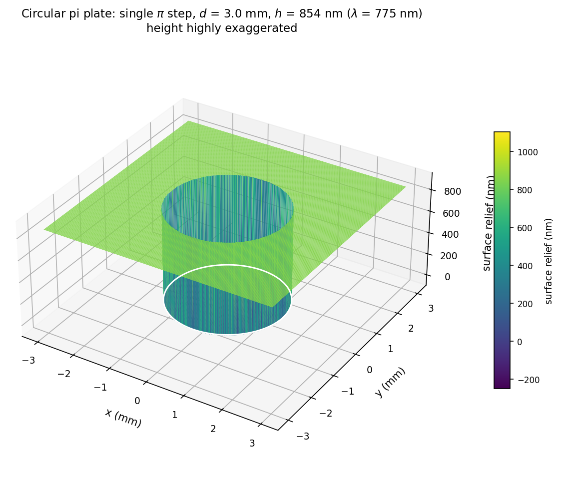
Schematic surface geometry of a circular pi plate
On the optical axis, every point of the pupil contributes with the same propagation phase, so the on-axis focal field is simply the sum of the transmitted field over the aperture. With a π step, the inner zone contributes with a minus sign. When the zone diameter is chosen so that the inner disc and the outer ring carry equal field contributions, the two terms cancel and the intensity at the focal point drops to zero. The energy is not lost, it is redistributed into two lobes that sit symmetrically above and below the focal plane along the optical axis, plus a faint lateral ring. This structure is called a bottle beam or, in the super-resolution community, a z-doughnut.
Circular pi plates and spiral phase plates are complementary rather than alternatives. A spiral phase plate produces a lateral null and confines the fluorescence in x and y, a circular pi plate produces an axial null and confines it in z. A 3D STED microscope therefore uses both, with the depletion power split between the two masks and the two beams recombined incoherently, so that the depletion patterns add in intensity rather than interfere. The power ratio between the xy-doughnut and the z-doughnut sets the aspect ratio of the effective PSF: all power on the vortex gives 2D STED, and a split of roughly 70:30 in favour of the vortex is a common starting point for a nearly isotropic 3D resolution.
Beyond 3D STED and MINFLUX, the axial null of a circular pi plate is used to build dark optical traps for cold atoms and nanoparticles, where the particle sits in the intensity minimum of a blue-detuned bottle beam and is confined in all three dimensions. The same element is used in laser material processing when a well-defined axial intensity profile is required, in depth-of-focus engineering, and in wavefront diagnostics as a defocus-sensitive phase mask.
How is the zone diameter chosen?
The zone diameter decides how deep the axial zero is, and it has to match the beam that illuminates the plate. The cancellation condition is that the field integrated over the inner disc equals the field integrated over the outer ring. For a Gaussian beam of 1/e² intensity diameter D this gives a closed-form answer:
d = D · √(ln 2) ≈ 0.83 · D
In other words, the diameter of the phase zone should be about 83 % of the 1/e² diameter of the beam. This is why we list four zone diameters for every wavelength: pick the one that matches the beam you already have, instead of building a telescope to match the plate. The table below gives the beam that each of our standard diameters is made for.
| Zone diameter d | Matched Gaussian beam, 1/e² diameter D | Matched Gaussian beam, 1/e² radius w | PN suffix |
|---|---|---|---|
0.2 mm | 0.24 mm | 0.12 mm | -200 |
1.0 mm | 1.20 mm | 0.60 mm | -1000 |
2.0 mm | 2.40 mm | 1.20 mm | -2000 |
3.0 mm | 3.60 mm | 1.80 mm | -3000 |
The design is forgiving: because the residual on-axis intensity scales with the square of the field imbalance between the two zones, a 1 % mismatch leaves only about 10-4 of the lobe peak on the axis. A beam that is a factor of two away from the design value, however, will visibly fill the axial zero. If none of the four standard diameters fits your beam, use the custom quote form below and give us the 1/e² diameter at the position of the plate.
Specifications
Substrate | optical grade fused silica |
Clear aperture | 10 mm (11x11x2.5 mm substrate) or 20 mm (22x22x2.5 mm substrate) |
Substrate thickness | 2.5 mm ± 0.1 mm |
Structure | single circular π step, binary (2 levels) |
Input beam | Gaussian |
Zone diameter d | 0.2 / 1.0 / 2.0 / 3.0 mm, tolerance ± 0.5 % |
Step height tolerance | ± 5 nm typical (± 0.02 rad phase error at 775 nm) |
Zone edge width | < 1 µm |
Surface quality | 40-20 scratch-dig |
Surface flatness | λ/10 over the clear aperture |
Transmission, uncoated | ≈ 93 %, Fresnel limited over both surfaces |
Coating | none as standard, AR coating on request |
Damage threshold | > 10 J/cm² at 1064 nm, 10 ns, uncoated (typical for fused silica) |
Residual on-axis intensity | < 10-3 of the lobe peak at the design wavelength |
Step height
The depth of the phase step follows directly from the requirement of a π phase shift in transmission, h = λ / [ 2 · (n(λ) − 1) ], with n(λ) the refractive index of fused silica. Since the index disperses only weakly, the step height is essentially proportional to the wavelength.
| λ | n (fused silica) | Step height h |
|---|---|---|
405 nm | 1.4696 | ≈ 431 nm |
488 nm | 1.4630 | ≈ 527 nm |
532 nm | 1.4607 | ≈ 577 nm |
592 nm | 1.4585 | ≈ 646 nm |
640 nm | 1.4570 | ≈ 700 nm |
660 nm | 1.4565 | ≈ 723 nm |
775 nm | 1.4537 | ≈ 854 nm |
780 nm | 1.4537 | ≈ 860 nm |
800 nm | 1.4533 | ≈ 882 nm |
1030 nm | 1.4502 | ≈ 1144 nm |
1064 nm | 1.4496 | ≈ 1183 nm |
Wavelength tolerance
If the plate is used at a wavelength other than the design wavelength, the step no longer produces exactly π and the axial null fills in. For a plate designed for λ0 and operated at λ0 + Δλ, the residual on-axis intensity relative to the lobe peak is approximately sin²( π Δλ / (2 λ0) ). A detuning of 1 % therefore leaves about 2.5 · 10-4 of the peak intensity on the axis, and a detuning of 5 % about 6 · 10-3. For STED depletion the practical rule is to stay within roughly 1 % of the design wavelength. For broadband or tunable sources, please contact us and we will pick the best compromise design wavelength.
Orientation and alignment
The plate is used in a collimated part of the beam, in a plane conjugate to the back pupil of the objective. Either side may face the source, the structured side is marked. Lateral decentring of the zone with respect to the beam axis is the dominant alignment error, since it breaks the radial symmetry and lifts the axial zero. Keep the decentring below about 1 % of the beam radius, which for a 2 mm beam diameter means better than 10 µm. Tip and tilt of the plate are uncritical up to a few degrees.
Application notes
1) Removing the cleaning / protective polymer
To ensure the protection and cleanliness of our products during shipping, we utilize a specialized optical grade polymer. Before using the optical elements in your setup, please remove the polymer from the surface using the provided sticker. For a detailed explanation, refer to this video by the polymer manufacturer:
2) Preparing the laser beam
The quality of the original laser beam is crucial for the depth of the axial zero after the phase plate. To ensure optimal quality, please employ spatial filtering for the original beam. In certain scenarios, a simplified variation of spatial filtering can be implemented:
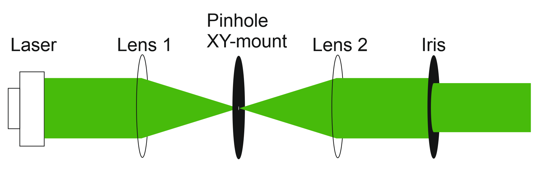
Spatial filtering is achieved by focusing the laser beam through a lens onto a pinhole, effectively removing spatial distortions and noise. Only the central, most coherent part of the beam passes through the pinhole, thereby improving its quality. A second lens is then used to recollimate the beam to the desired diameter, and an additional iris can be employed to remove remaining higher-order diffractions.
3) Matching the zone diameter to your beam
Measure the 1/e² diameter D of the collimated beam at the position of the plate and pick the zone diameter closest to d = 0.83 · D. Our four standard zones cover 1/e² beam diameters of roughly 0.24 mm (d = 0.2 mm), 1.2 mm (d = 1.0 mm), 2.4 mm (d = 2.0 mm) and 3.6 mm (d = 3.0 mm). If the beam is much larger than the design value, the outer ring is over-weighted and the axial zero fills in; if it is much smaller, the inner zone dominates. In both cases the lobes also become asymmetric.
4) Combining the z-doughnut with the xy-doughnut for 3D STED
Split the depletion beam into two arms, place a spiral phase plate in one and a circular pi plate in the other, then recombine the arms with orthogonal polarizations or with a delay longer than the coherence length, so that the two depletion patterns add in intensity and do not interfere. A half-wave plate in front of the splitting element tunes the power ratio between the two arms; that ratio, not the plates themselves, is what you adjust to trade lateral against axial resolution. Convert to circular polarization after recombination, with the handedness matched to the sign of the vortex, otherwise the lateral null of the spiral phase plate will not close under a high-NA objective.
5) Verifying the null
Image the focus with a scattering gold bead or a mirror scan and record an xz section. A good z-doughnut shows two lobes of equal brightness separated along the axis, with a dark plane between them. Asymmetric lobes point to spherical aberration or a defocused conjugate plane; a filled-in centre points to a beam diameter that does not match the zone diameter, a decentred plate, or a wavelength offset, in that order of likelihood.